I have been thinking of developing a ogg vorbis audio decoder core (not a real time version that I am intending to work on at this moment; but simply a offline decoder) on my Avnet Spartan 3A evaluation board that I purchased a few months back. On an introductory note, this eval kit is really low cost (costs 39$) and has quite a lot of features to play with. I can say the evaluation board is simply great!

I decided to use the SPI flash memory from Spansion for storing the raw audio packets; due to the large memory storage. This board also comes with another parallel flash but only 32 Mega bits. I have been meaning to use this to store the FPGA configuration file; which will be quite large once I start working on the decoder core.
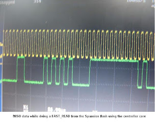
For the past few days, I was onto developing a SPI controller core in verilog for the Spansion memory (used in the board). By default configuration, it can be accessed via SPI controller module on the Cypress pSoC. But I decided to write my own core owing to 2 reasons; the SCLK on the pSOC seemed to be of the order of few KHz and the data communication mode between the FPGA and Cypress is either UART (obviously very slow) or SPI; which warrants a SPI Master Slave device on the FPGA if I intend to use SPI.

I have so far successfully developed the backend (or backbone) core which will generate the necessary signals. Today I wrote a small front end code to write 5 data bytes starting on a pre-destined address location (Hex 50000 till 50005) by touching capsense button "Push_A".

I, then, read back the values from the same 5 locations by touching capsense button "Push_B" and indicate it on the LED with a "1010" pattern if it is successful; otherwise the LEDs will be blinking.


Also, I did a bulk erase of the chip by touching capsense button "Push_C" which took around 1 min 8 seconds (safely can assume between 1 to 2 minutes which matches with the datasheet spec). I also read back the data from the same locations as before and the test failed as expected.


I am able to do most of the required operations that we want to do on a flash memory using the FPGA and the custom core. There are some open source cores available for SPI master. But I wanted to design my own one; this has given me enough confidence in working on more complex designs which I am intending to in the coming days.
I would be designing a proper front-end code; with an UART to SPI interface next. Inputs and feedbacks are most welcome!
Links for the source files for this initial revision:
http://www.2shared.com/file/5435094/4490a724/SPI_Core.html
http://www.2shared.com/file/5435095/339797b2/SPI_Mast_Mod.html
http://www.2shared.com/file/5435096/aa9ec608/SPI_Master_BackBone.html